The Evolution of Semiconductor Packaging: Innovations That Shape the Future
The modern electronics industry continues to push the boundaries of speed, size, and performance. From smartphones to satellites, the demand for reliable, high-frequency devices is rising fast. To meet this challenge, engineers are constantly improving the design and materials used in semiconductor packaging. What was once a simple protective case for a chip has now evolved into a crucial part of overall device performance. Packaging solutions today need to support high thermal loads, protect against environmental factors, and ensure minimal signal loss.
This approach stands out due to its ability to reduce parasitic effects and support excellent thermal conductivity. Engineers working on RF (radio frequency), microwave, and millimeter-wave systems are particularly interested in this technology because it helps maintain signal integrity in extreme environments. These types of applications require packaging that not only protects the chip but also supports its function at high performance levels.
The Role of Advanced Packaging in Electronics
The importance of packaging goes beyond physical protection. In high-speed electronic systems, packaging affects signal transmission, power handling, and heat dissipation. As frequencies increase, even small amounts of resistance or interference can lead to performance losses.Among the wide range of packaging solutions available, air cavity package technology is gaining more attention for its role in high-frequency and high-power applications. That’s why modern packaging materials and designs are tailored to meet the specific needs of each device, especially in RF applications. Engineers must consider how every component will behave under different thermal, mechanical, and electrical stresses.
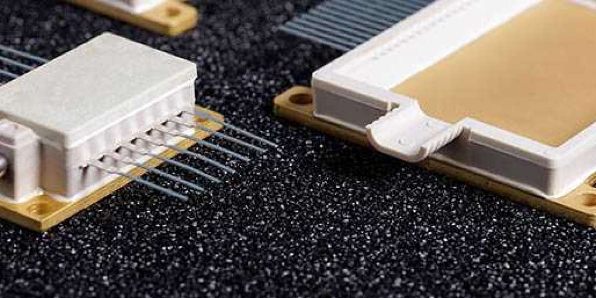
Traditional packaging methods often fall short when faced with these challenges. Plastic encapsulated packages, while inexpensive and easy to produce, may introduce unwanted interference or degrade signal performance. On the other hand, metal-ceramic packages offer improved shielding but may not be suitable for every layout or thermal requirement. These limitations have created a demand for more flexible and effective packaging options that can balance cost, performance, and manufacturability.
Material Science and Thermal Management
One of the key issues in electronic packaging is thermal management. As chips become smaller and more powerful, they generate more heat in a smaller area. Without proper heat dissipation, performance will degrade and component lifetimes will shorten. Engineers are now turning to materials with higher thermal conductivity, such as aluminum nitride or copper-molybdenum composites, to help draw heat away from critical components.
The mechanical properties of packaging materials are also crucial. They need to maintain a reliable seal over time, even under stress from temperature fluctuations or vibration. In many cases, the right combination of metals, ceramics, and adhesives ensures the package stays intact and performs reliably throughout its lifecycle. Manufacturers are also exploring materials that reduce moisture penetration, another major factor that can lead to device failure over time.
RF and Microwave Device Demands
Packaging high-frequency devices presents additional challenges. At RF and microwave frequencies, even tiny structural variations in the package can introduce impedance mismatches or reflection issues. Signal losses become more critical, and electromagnetic interference is harder to manage. Engineers must design packages that provide both protection and performance, which means tightly controlling the geometry and internal structure of the package.
This is where innovations in design are making a major impact. Engineers are increasingly using simulation tools to model how a signal will behave inside a package before it is even manufactured. This allows for more accurate design and fewer iterations during prototyping. They can optimize the shape, size, and material selection to achieve the desired electrical and thermal characteristics without compromising reliability.
Design Flexibility for Custom Applications
Modern packaging solutions also allow for greater customization. Designers working in aerospace, defense, and telecommunications often have very specific requirements that standard packages cannot meet. They may need to accommodate non-standard pin configurations, integrate passive components inside the package, or design for specific thermal performance levels. In these cases, custom-designed packages are created from the ground up to meet the unique demands of the application.
The ability to create low-volume, high-performance packaging solutions is critical for industries that operate in extreme conditions. These packages must pass rigorous testing and comply with strict reliability standards. As a result, manufacturers have invested in new manufacturing techniques such as precision machining, advanced joining methods, and cleanroom-based assembly processes to ensure quality and consistency at every step.
How Air Cavity Designs Improve Performance
In high-frequency applications, the dielectric environment inside the package plays a significant role in signal behavior. Solid plastic or epoxy encapsulants can introduce dielectric losses or alter signal propagation. By contrast, an air cavity provides a low-loss medium that better preserves signal integrity. This results in less power loss and improved overall device efficiency.
Another major benefit of this approach is improved heat dissipation. Because air does not retain heat like solid materials, it helps prevent thermal buildup inside the package. Combined with thermally conductive materials used in the package base, this design helps ensure consistent thermal performance even under heavy operating loads. As frequencies increase into the millimeter-wave range, these advantages become even more critical to maintaining stable, high-performance systems.
In the middle of this technological shift, air cavity package technology has proven itself as a valuable solution. It supports high-frequency designs without introducing excess loss or distortion. Its mechanical simplicity and ease of customization make it a strong choice for designers who need flexibility and performance. With proven applications across 5G infrastructure, satellite communications, radar systems, and more, it’s clear that this approach will play a significant role in the future of electronics packaging.
Reliability in Harsh Environments
Devices used in aerospace, defense, and space environments are often exposed to extreme temperatures, pressure changes, and vibration. In these conditions, the packaging must maintain integrity without compromising performance. Metal and ceramic-based packages, especially those using air cavities, offer the structural strength and environmental protection needed for these missions.
Hermetic sealing is another major requirement. Moisture and contaminants can cause corrosion or electrical shorts, especially in sensitive RF devices. Air cavity packages can be hermetically sealed to prevent these issues, helping ensure long-term reliability even in the harshest settings. Proper sealing also supports compliance with military and aerospace standards, which are often more demanding than commercial ones.
Integration with Modern Manufacturing
Scalability is essential in any technology, and packaging is no exception. While many advanced packages begin as low-volume, custom solutions, they must also be scalable for broader use. Fortunately, developments in automated assembly and inspection have made it easier to manufacture high-performance packages at higher volumes. Manufacturers can now maintain tight quality control while increasing production capacity.
Designers also benefit from better interoperability with standard PCB manufacturing techniques. As new materials and designs are developed, they are optimized to work with existing assembly lines. This reduces the need for costly adjustments or special processes and shortens the time from design to deployment. By combining performance with manufacturability, the industry can respond faster to changing demands.
Looking Ahead: Packaging Trends to Watch
The future of electronic packaging will likely bring even more integration. As components continue to shrink and systems become more complex, the package will play a larger role in determining system performance. Technologies like 3D packaging, system-in-package (SiP), and heterogeneous integration are already changing how devices are built and connected. Each of these trends will require new materials, new designs, and new ways of thinking about packaging.
There is also growing interest in sustainability. Eco-friendly materials, recyclable components, and energy-efficient manufacturing processes are becoming part of the conversation. As companies aim to reduce their environmental footprint, they will look for packaging solutions that align with these goals without sacrificing performance or reliability.
In this fast-moving landscape, air cavity package technology remains a trusted solution for high-performance, high-frequency applications. Its unique combination of signal integrity, thermal efficiency, and design flexibility makes it ideal for industries that demand the highest levels of reliability. As engineers continue to innovate, this technology will remain a vital part of the electronics ecosystem for years to come.