" Electron Beam Lithography Market - Overview, Size, Share, Industry Trends and Opportunities
Global Electron Beam Lithography Market Segmentation, By Type (Gaussian Beam EBL Systems and Shaped Beam EBL Systems), Application (Academic Field, Industrial Field, and Others) – and Industry Trends
Access Full 350 Pages PDF Report @
https://www.databridgemarketresearch.com/reports/global-electron-beam-lithography-market
**Segments**
- **By Type**: The global electron beam lithography market can be segmented by type into scanning E-beam lithography and variable-shaped E-beam lithography. Scanning E-beam lithography involves moving the focused electron beam across the surface of the substrate to create the desired pattern. On the other hand, variable-shaped E-beam lithography utilizes a shaped beam to directly write the pattern onto the substrate, offering higher precision and throughput. Both types play a crucial role in fulfilling the diverse requirements of various industries such as semiconductor, electronics, and biomedical.
- **By Application**: The market can also be segmented by application, including semiconductor manufacturing, photonics, optoelectronics, MEMS (Micro-Electro-Mechanical Systems), and nanotechnology. Electron beam lithography is widely employed in semiconductor manufacturing for the production of integrated circuits with nanoscale features. Moreover, its applications in photonics, optoelectronics, MEMS, and nanotechnology further widen its scope across different sectors, driving market growth.
- **By End-Use Industry**: Based on end-use industry, the global electron beam lithography market is segmented into semiconductor, research institutions, and others. The semiconductor industry accounts for a significant share of the market due to the increasing demand for high-resolution patterning technologies in the production of advanced microchips and electronic components. Research institutions also play a key role in driving market growth by leveraging electron beam lithography for fundamental research in nanotechnology and other fields.
**Market Players**
- **Raith GmbH**: Raith GmbH is a prominent player in the global electron beam lithography market known for offering high-performance E-beam lithography systems tailored for nanofabrication applications. The company's cutting-edge solutions cater to diverse requirements in research, academia, and industrial settings, positioning it as a key player in the market.
- **Vistec Electron Beam GmbH**: Vistec Electron Beam GmbH is another leading market player specializing in advanced electron beam lithography systems for nanotechnology and semiconductor applications. With a strong focus on innovation and technology development, Vistec Electron Beam GmbH remains at the forefront of driving technological advancements in the field of E-beam lithography.
- **NanoBeam Limited**: NanoBeam Limited is recognized for its compact and versatile electron beam lithography systems designed for rapid prototyping and low-volume production in various industries. The company's emphasis on user-friendly solutions and customized offerings has garnered significant attention in the market, contributing to its competitive position.
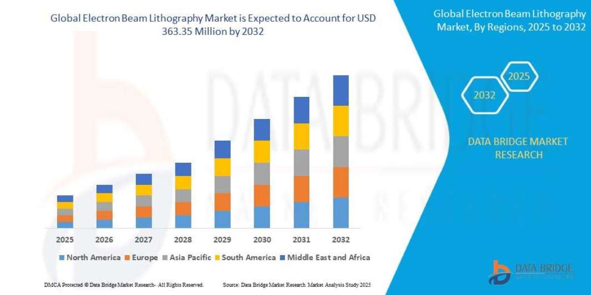
The global electron beam lithography market is poised for substantial growth, driven by the increasing demand for high-resolution patterning technologies across diverse industries. Factors such as technological advancements, rising investments in RD activities, and the expansion of semiconductor manufacturing capabilities are expected to propel market expansion in the coming years.
https://www.databridgemarketresearch.com/reports/global-electron-beam-lithography-marketThe global electron beam lithography market is experiencing a significant upward trajectory driven by several key factors. One notable trend shaping the market landscape is the increasing adoption of electron beam lithography technology across various industries. The semiconductor sector, in particular, is a major driver of market growth, with the demand for high-resolution patterning technologies escalating in the production of advanced microchips and electronic components. As the need for smaller, more intricate designs continues to grow, the role of electron beam lithography in enabling nanoscale manufacturing processes becomes increasingly vital.
Furthermore, the market is witnessing a surge in research and development activities in sectors such as photonics, optoelectronics, MEMS, and nanotechnology. These industries rely on electron beam lithography for intricate patterning and fabrication processes, driving the demand for advanced lithography systems. Research institutions also contribute significantly to market growth by utilizing electron beam lithography for fundamental research in nanotechnology and other cutting-edge fields. As collaboration between industry and academia intensifies, the market is likely to witness further advancements in lithography technology and applications.
In terms of market players, companies like Raith GmbH, Vistec Electron Beam GmbH, and NanoBeam Limited are at the forefront of driving innovation and technology development in the electron beam lithography market. These key players offer a diverse range of lithography systems tailored to meet the specific needs of various industries, including nanofabrication, semiconductor manufacturing, and rapid prototyping. Their focus on high-performance solutions, user-friendly interfaces, and customization options sets them apart in a competitive market environment.
Looking ahead, the future growth prospects of the electron beam lithography market appear promising, fueled by ongoing technological advancements and increased investments in research and development. The expansion of semiconductor manufacturing capabilities, coupled with the growing demand for nanoscale patterning solutions, is expected to drive further market expansion in the coming years. As industries continue to prioritize precision, efficiency, and innovation in their manufacturing processes, electron beam lithography is poised to play a pivotal role in shaping the next generation of cutting-edge technologies and products.**Segments**
- Global Electron Beam Lithography Market Segmentation, By Type: Gaussian Beam EBL Systems and Shaped Beam EBL Systems
- Global Electron Beam Lithography Market Segmentation, By Application: Academic Field, Industrial Field, and Others
The global electron beam lithography market is witnessing significant growth propelled by the expanding adoption of electron beam lithography technology across various industries. The semiconductor sector stands out as a major catalyst for market expansion as the demand for high-resolution patterning technologies rises in the production of advanced microchips and electronic components. As the need for intricate designs on a smaller scale continues to increase, the role of electron beam lithography becomes increasingly crucial in enabling nanoscale manufacturing processes.
Moreover, the market is experiencing a surge in research and development activities in sectors like photonics, optoelectronics, MEMS, and nanotechnology, all of which heavily rely on electron beam lithography for intricate patterning and fabrication processes. This growing demand for advanced lithography systems in these industries is fueling market growth. Additionally, research institutions are playing a vital role in driving market expansion by utilizing electron beam lithography for fundamental research in cutting-edge fields such as nanotechnology. The collaboration between industry and academia is expected to lead to further advancements in lithography technology and its applications.
Key players such as Raith GmbH, Vistec Electron Beam GmbH, and NanoBeam Limited are leading the way in driving innovation and technological development in the electron beam lithography market. These companies offer a diverse range of lithography systems tailored to meet the specific needs of various industries, including nanofabrication, semiconductor manufacturing, and rapid prototyping. Their focus on high-performance solutions, user-friendly interfaces, and customization options sets them apart in a competitive market environment.
Looking ahead, the future growth prospects of the electron beam lithography market appear promising, driven by ongoing technological advancements and increased investments in research and development. The expansion of semiconductor manufacturing capabilities, coupled with the growing demand for nanoscale patterning solutions, is expected to fuel further market expansion in the coming years. As industries continue to prioritize precision, efficiency, and innovation in their manufacturing processes, electron beam lithography is set to play a pivotal role in shaping the next generation of cutting-edge technologies and products.
Key Coverage in the Electron Beam Lithography Market Report:
- Detailed analysis of Global Electron Beam Lithography Market by a thorough assessment of the technology, product type, application, and other key segments of the report
- Qualitative and quantitative analysis of the market along with calculation for the forecast period
- Investigative study of the market dynamics including drivers, opportunities, restraints, and limitations that can influence the market growth
- Comprehensive analysis of the regions of the Electron Beam Lithography industry and their futuristic growth outlook
- Competitive landscape benchmarking with key coverage of company profiles, product portfolio, and business expansion strategies
Table of Content:
Part 01: Executive Summary
Part 02: Scope of the Report
Part 03: Global Electron Beam Lithography Market Landscape
Part 04: Global Electron Beam Lithography Market Sizing
Part 05: Global Electron Beam Lithography Market by Product
Part 06: Five Forces Analysis
Part 07: Customer Landscape
Part 08: Geographic Landscape
Part 09: Decision Framework
Part 10: Drivers and Challenges
Part 11: Market Trends
Part 12: Vendor Landscape
Part 13: Vendor Analysis
Reasons to Buy:
- Review the scope of the Electron Beam Lithography Market with recent trends and SWOT analysis.
- Outline of market dynamics coupled with market growth effects in coming years.
- Electron Beam Lithography Market segmentation analysis includes qualitative and quantitative research, including the impact of economic and non-economic aspects.
- Regional and country level analysis combining Electron Beam Lithography Market and supply forces that are affecting the growth of the market.
- Market value data (millions of US dollars) and volume (millions of units) for each segment and sub-segment.
- and strategies adopted by the players in the last five years.
Browse Trending Reports:
Medical Electrodes Market
Hyper-Converged Infrastructure Market
Homecare Surgical Drains Market
Kombucha Market
Metallic Pigments Market
Robotics in Drug Discovery Market
Mitogen-Activated ERK Kinase (MEK) Inhibitors Market
Input Method Editor Software Market
Zinc Citrate Market
Specialty Nitrile Butadiene Rubber Market
Aloe Vera Juice Market
Digital Photo Frames Market
About Data Bridge Market Research:
Data Bridge set forth itself as an unconventional and neoteric Market research and consulting firm with unparalleled level of resilience and integrated approaches. We are determined to unearth the best market opportunities and foster efficient information for your business to thrive in the market. Data Bridge endeavors to provide appropriate solutions to the complex business challenges and initiates an effortless decision-making process.
Contact Us:
Data Bridge Market Research
US: +1 614 591 3140
UK: +44 845 154 9652
APAC : +653 1251 975